Common Design Mistakes in 8 Layer PCB
Introduction
As electronic products continue to demand higher performance, smaller form factors, and improved signal integrity, 8 layer PCBs have become a common solution in industrial, automotive, communication, and high-speed digital applications.
However, increasing layer count also significantly increases design complexity. Many reliability and yield problems in 8 layer PCB fabrication originate not from manufacturing defects, but from early design mistakes that overlook real manufacturing constraints.
This article reviews the most common design mistakes in 8 layer PCB, explains why they occur, and shows how experienced PCB manufacturers help prevent these issues through DFM expertise and process control.
PCB Instant Quote
.my-button {
display: inline-block;
padding: 10px 50px;
font-size: 16px;
text-align: center;
text-decoration: none;
background-color: blue;
color: #fffff0;
border: none;
border-radius: 5px;
font-weight: bold;
cursor: pointer;
box-shadow: 0px 2px 5px rgba(0, 0, 0, 0.3);
transition: background-color 0.3s ease, transform 0.3s ease;
}
.my-button:hover {
background-color: #C23C30;
transform: scale(1.05);
}
Why 8 Layer PCB Design Is More Challenging?
Compared to low-layer boards, 8 layer PCBs introduce:
Complex stackup structures
Tighter registration and drilling tolerances
Higher sensitivity to thermal and mechanical stress
Stronger coupling between design decisions and fabrication processes
Without proper coordination between design and manufacturing, small design oversights can lead to warpage, delamination, via failure, or low production yield.
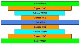
Mistake 1: Unbalanced Layer Stackup
One of the most common design mistakes in 8 layer PCB is an unbalanced stackup.
Typical problems include:
Asymmetrical copper distribution
Uneven dielectric thickness between layers
Signal layers concentrated on one side
Consequences:
Board warpage during lamination
Increased risk of delamination
Registration issues between inner layers
Manufacturing perspective:
Professional manufacturers review stackups to ensure mechanical symmetry and copper balance, reducing stress during lamination and thermal cycling.
Mistake 2: Incorrect Via Structure Selection
Designers often overuse standard through-hole vias without considering:
Aspect ratio limitations
Via reliability under thermal stress
Signal integrity and routing efficiency
In 8 layer PCBs, poor via choices can cause:
Thin or uneven copper plating
Via barrel cracking
Reduced yield during drilling and plating
Best practice:
Select via structures (through, blind, buried) based on layer usage, thickness, and manufacturing capability, not only routing convenience.
Mistake 3: Inadequate Power and Ground Plane Design
Power and ground planes play a critical role in signal integrity and thermal performance.
Common errors include:
Fragmented reference planes
Insufficient copper continuity
Poor return path planning
Results:
Increased EMI
Signal noise and impedance instability
Localized heating
Manufacturers often identify these issues during DFM review and recommend continuous plane structures and optimized layer pairing.
Mistake 4: Ignoring Copper Balance Across Layers
Large copper areas on some layers and sparse copper on others can disrupt lamination pressure and resin flow.
Potential risks:
Inner layer shift
Resin starvation or excess resin areas
Board thickness inconsistency
Manufacturers mitigate this by:
Copper balancing techniques
Panel layout optimization
Adjusted lamination parameters
Mistake 5: Trace Width and Spacing Below Manufacturing Limits
Designing traces too close to minimum limits may pass CAD rules but fail in real production.
Issues include:
Inner layer over-etching
Reduced copper thickness
Lower electrical reliability
Key insight:
Inner layers experience different etching behavior than outer layers, requiring process-aware trace design.
Mistake 6: Poor Thermal Management Design
8 layer PCBs often handle higher power densities, yet designers may neglect:
Thermal vias
Heat spreading copper
Thermal expansion mismatch
This can result in:
Localized overheating
Via fatigue
Long-term reliability degradation
Manufacturers help by evaluating thermal paths and material selection, especially for high-temperature applications.
Mistake 7: Insufficient Via-to-Plane and Via-to-Edge Clearance
Ignoring IPC recommendations or manufacturing tolerances may cause:
Via breakout
Shorts between layers
Electrical failures after thermal cycling
Accurate clearance design must account for drilling accuracy, layer registration, and plating growth.
Mistake 8: Lack of Assembly Process Consideration
Designs optimized only for fabrication may fail during assembly.
Common oversights:
Via-in-pad without proper filling
Pads incompatible with lead-free reflow
No allowance for multiple reflow cycles
Experienced manufacturers evaluate designs with fabrication and assembly compatibility in mind.
How Manufacturers Help Prevent These Design Mistakes?
Professional PCB manufacturers reduce design risk by offering:
Early DFM and stackup consultation
Material and process compatibility checks
Via and drilling capability alignment
Prototyping feedback before mass production
This collaboration significantly improves yield, reliability, and time-to-market.
PCBBUY’s Experience with 8 Layer PCB Manufacturing
With extensive experience in multilayer PCB fabrication, PCBBUY supports complex 8 layer PCB projects through:
Optimized stackup and copper balance control
Precise drilling and via plating processes
Strict lamination and thermal reliability management
Comprehensive DFM review before production
These capabilities help customers avoid common design mistakes and achieve stable, repeatable quality.
Conclusion
Designing an 8 layer PCB requires more than routing density and electrical performance considerations.Understanding manufacturing realities is essential to avoid costly failures and delays.
By recognizing common design mistakes in 8 layer PCB and working closely with an experienced manufacturer, designers can significantly improve product reliability and manufacturing success.
FAQ
What are the most common design mistakes in 8 layer PCB?
Unbalanced stackups, poor via selection, inadequate copper balance, and ignoring manufacturing tolerances are among the most common issues.
Why is stackup design critical for 8 layer PCB?
Stackup affects mechanical stability, thermal behavior, signal integrity, and lamination quality. Poor stackup design often leads to warpage or delamination.
Can PCB manufacturers help fix design mistakes?
Yes. Experienced manufacturers provide DFM reviews, stackup optimization, and process-based feedback before production.
How does copper balance affect PCB manufacturing?
Copper imbalance can cause resin flow issues, inner layer shift, and board warpage during lamination.
Why is DFM important for 8 layer PCB projects?
DFM ensures the design aligns with real manufacturing capabilities, improving yield, reliability, and overall production efficiency.
PCB Knowledge ⋅ 01/29/2026 09:41